AI, The electronics industry has long relied on the principle of packing ever-smaller transistors onto the surface of a single computer chip to achieve faster and more efficient devices. However, as we approach the physical limits of this strategy, chip manufacturers are exploring new dimensions — literally.

Rather than expanding outwards, the industry is now looking upwards. The idea is to stack multiple layers of transistors and semiconducting elements, transforming chip designs from sprawling ranch houses to high-rise towers. These multilayered chips promise exponentially greater data processing capabilities and the ability to perform more complex functions than today’s electronics.
Overcoming the Silicon Barrier
One of the biggest challenges in developing stackable chips is the foundational material. Silicon wafers, currently the go-to platform for chip manufacturing, are thick and bulky. Each layer of a stacked chip built on silicon requires additional silicon “flooring,” which slows communication between layers.
Now, engineers at MIT have developed a revolutionary solution. In a recent study, the team unveiled a multilayered chip design that eliminates the need for silicon wafer substrates. Even better, their approach works at low temperatures, preserving the delicate circuitry of underlying layers.
This new method allows high-performance semiconducting materials to be grown directly on each other, without requiring silicon wafers as a scaffold. The result? Faster and more efficient communication between layers and a significant leap forward in computing potential.
A New Method for a New Era
The breakthrough leverages a process developed by the MIT team to grow high-quality semiconducting materials, specifically transition-metal dichalcogenides (TMDs). TMDs, a type of 2D material, are considered a promising successor to silicon due to their ability to maintain semiconducting properties at atomic scales. Unlike silicon, whose performance degrades as it shrinks, TMDs hold their own.
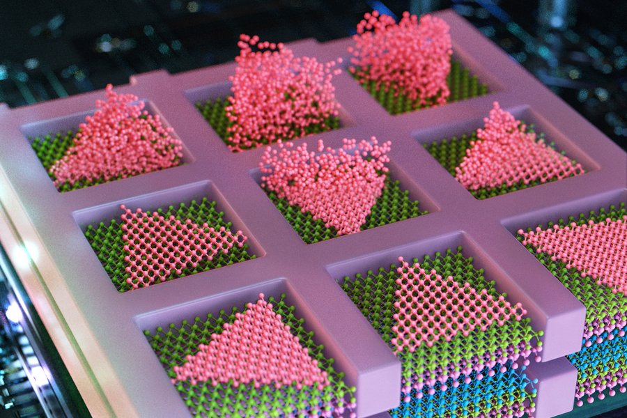
Previously, the team grew TMDs on silicon wafers using a patterned silicon dioxide mask. Tiny openings in the mask acted as “seed pockets,” encouraging atoms to arrange themselves in orderly, single-crystalline structures. However, this process required temperatures around 900°C, which would destroy a chip’s underlying circuitry.
The team fine-tuned this method in their latest work, borrowing insights from metallurgy. They discovered that nucleation — the initial formation of crystals — requires less energy and heat when it begins at the edges of a mold. Applying this principle, they managed to grow TMDs at temperatures as low as 380°C, preserving the integrity of the circuitry below.
Building Multilayered Chips
Using this low-temperature process, the researchers successfully fabricated a multilayered chip with alternating layers of two TMDs: molybdenum disulfide (ideal for n-type transistors) and tungsten diselenide (suitable for p-type transistors). These materials were grown in single-crystalline form, directly on each other, without silicon wafers in between.
This method effectively doubles the density of semiconducting elements on a chip. Furthermore, it enables the creation of metal-oxide-semiconductor (CMOS) structures—the building blocks of modern logic circuits—in a true 3D configuration. Unlike conventional 3D chips, which require drilling through silicon wafers to connect layers, this growth-based approach allows for seamless vertical alignment and higher yields.
A Future of AI-Powered Devices
The potential applications of this technology are groundbreaking. The team envisions using these stackable chips to power AI hardware for laptops, wearables, and other devices, delivering supercomputer-level performance in a compact form. Such chips could also store massive amounts of data, rivaling the capacity of physical data centers.
“This breakthrough opens up enormous potential for the semiconductor industry,” says Jeehwan Kim, associate professor of mechanical engineering at MIT and senior author of the study. “It could lead to orders-of-magnitude improvements in computing power for AI, logic, and memory applications.”
From Concept to Commercialization
Kim has launched a startup called FS2 (Future Semiconductor 2D materials) to scale up and commercialize this innovation. While the current demonstration is at a small scale, the next step is to develop fully operational AI chips using this technology.